


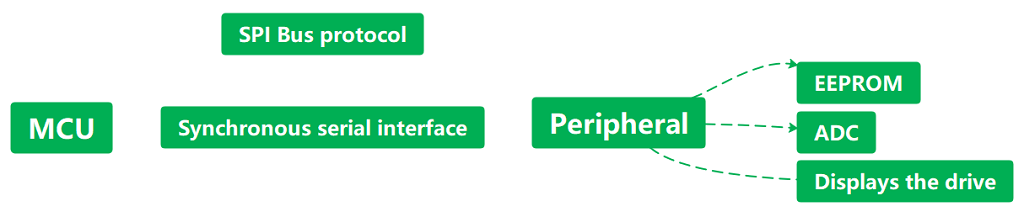
SPI, known as Serial Peripheral Interface, is a high-speed, full-duplex, synchronous communication bus.

It works in a master-slave mode, in which a master device is usually used for one or more slave devices.

4 wires are required for bi-directional data transfer, 3 wires can be cut for uni-directional data transfer.


This pin corresponds to the master device data sending pin and the slave device data receiving pin.


This pin corresponds to the master device data receiving pin and the slave device data sending pin.
SCLK – synchronous clock, usually output by the master device.

Slave selection, which is used to select a slave device, allows the master device to communicate with a specific slave device to avoid conflicts on the data line.

SPI does not specify a maximum speed, the communication rate is determined solely by the capabilities of the two communicating parties.

Therefore, the use of SPI requires consulting the data sheets of both parties and adjusting the communication rate to the actual situation.
The SPI bus protocol was first introduced by Motorola as a synchronous serial interface.
Due to its simplicity, performance, and lack of patent implications, the SPI bus protocol was first introduced by Motorola as a synchronous serial interface.

The interface is therefore supported by many manufacturers’ devices and is widely used in MCUs and peripheral modules.
It is widely used in MCUs and peripheral modules such as E2PROMs, ADCs, display drivers, etc.
It is important to note that the SPI interface is a de facto standard.
Most manufacturers have based their designs on Motorola’s definition of the SPI interface, and many variants have been derived from it.
As a result, the SPI interface of different manufacturers’ products may vary somewhat in use.
Some of them cannot be interconnected directly (requiring the necessary software modifications), so in practice, it is necessary to read the manufacturer’s documentation carefully to confirm this.
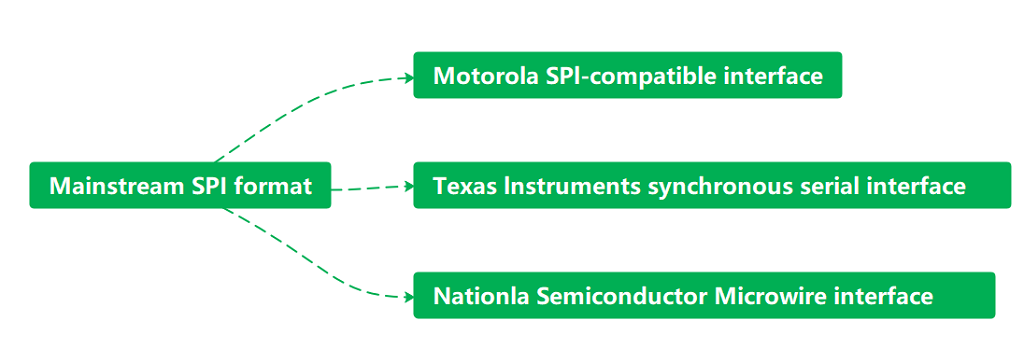
The main SPI formats available today are Motorola, Texas Instruments and National Semiconductor.
The most common format is the Motorola SPI format, so we will focus on the Motorola SPI format.

The main features of the Motorola SPI format are:
The state and phase of the synchronous clock at idle can be controlled by configuring the clock polarity and clock phase.
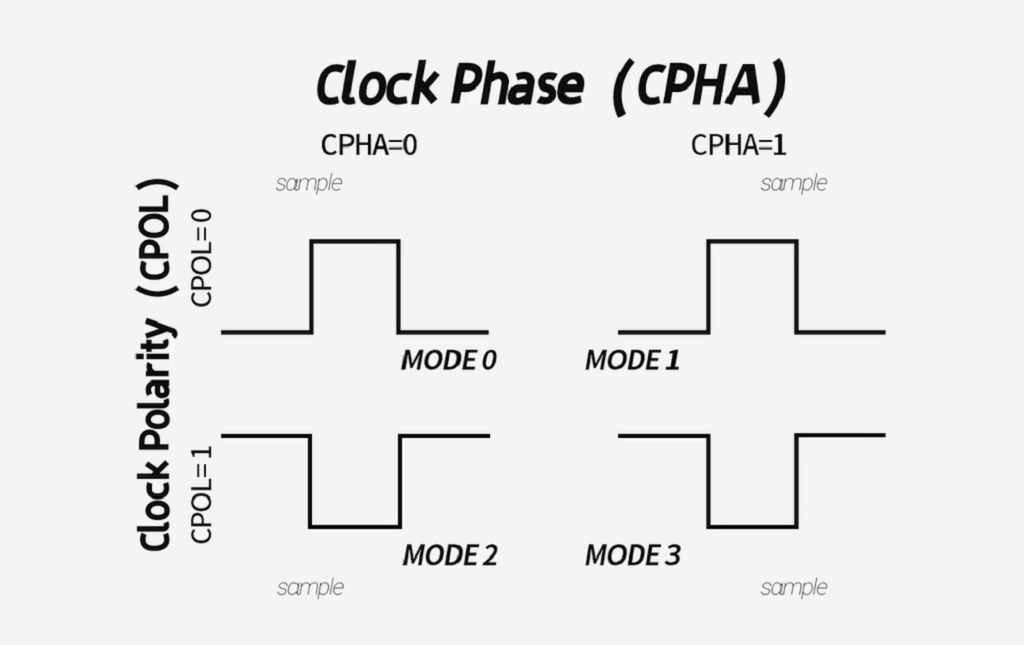
Clock Polarity: The level of the clock signal when idle, if the clock polarity is low,
If the clock polarity is low, then the clock signal pin will output a low level when idle, and vice versa.
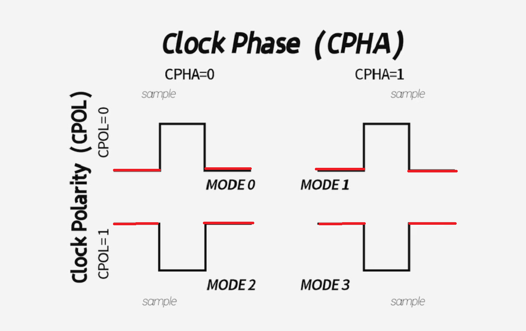
Clock Phase: Selects the clock edge on which the data is captured, if the clock phase is low,
If the clock phase is low, then the data is captured on the first clock edge. If the clock phase is low, the data is captured on the first clock edge, and vice versa, the data is captured on the second clock edge.
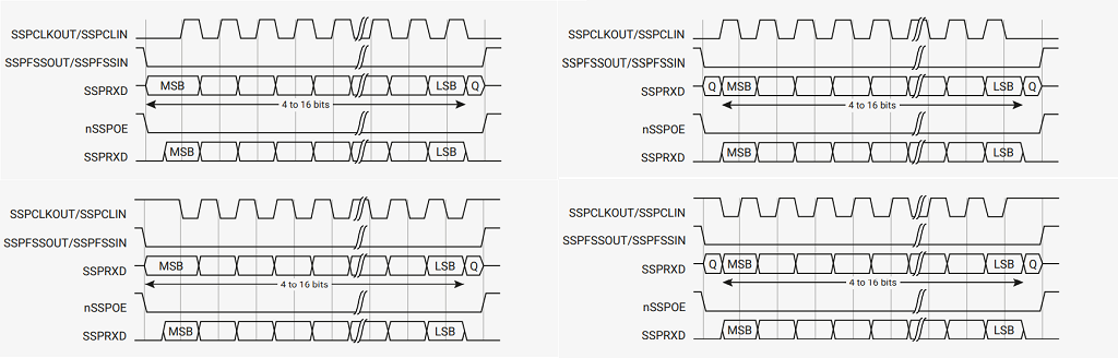
The above four diagrams show the data transmission under different clock polarity and clock phase conditions
The RP2040 has two identical SPI controllers, both based on the ARM Primecell Synchronous Serial Port (SSP) (PL022).
We will use them later to explain the SP| parameters, and now we see the main SPI parameters of the RP2040.
1. Master-slave mode support (supports the three main SPI’s).
2. 8 unit depth transceiver FIFOs (8 deep TX and RX FIFOs).
3. Interrupt generator can serve FIFO memory or error markers.
5. DMA driver can be used.
6. Programmable clock.
7. Programmable data size (4-16bit).
Now we see the logic block diagram of the RP2040, the SPI logic block diagram is closer to the UART logic block diagram.
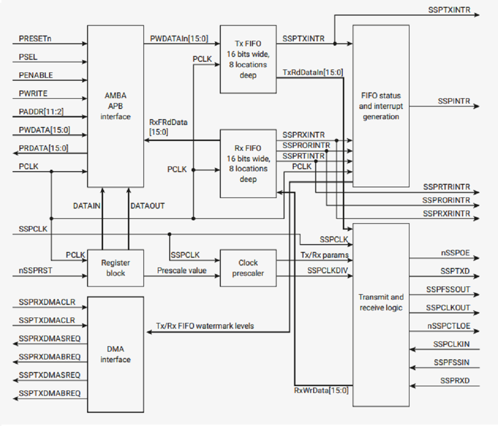
This is just an introduction to what each part does.
Used to access status and control registers and to transfer data. and to receive FIFO memory.
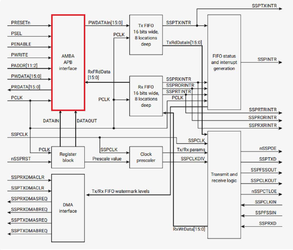
Data is written or read via the AMBA APB interface.
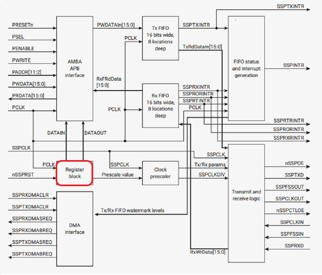
Consists of two free-running, reloadable counters.
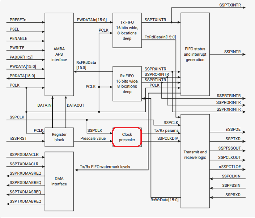
Consists of two free-running, reloadable counters.
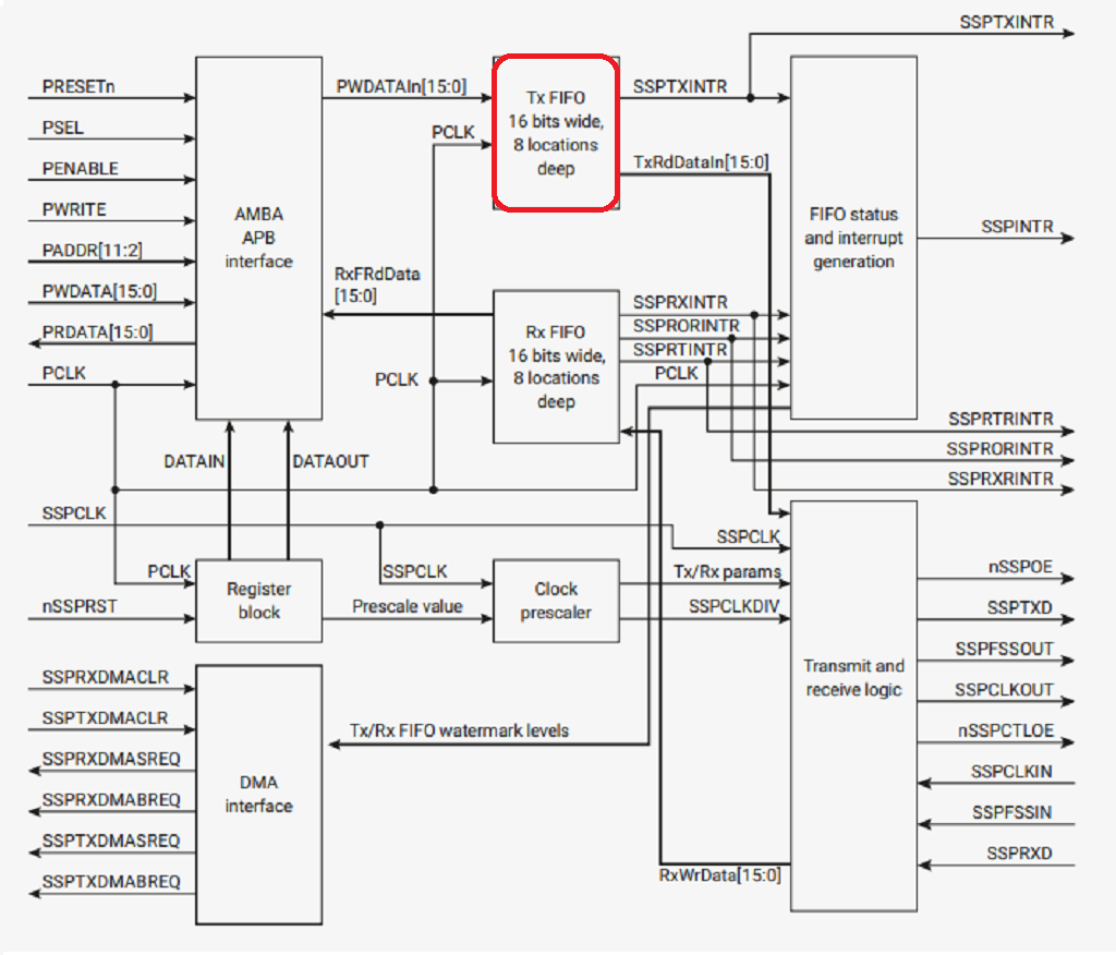
It is a 16-bit wide, 8-bit deep memory buffer.
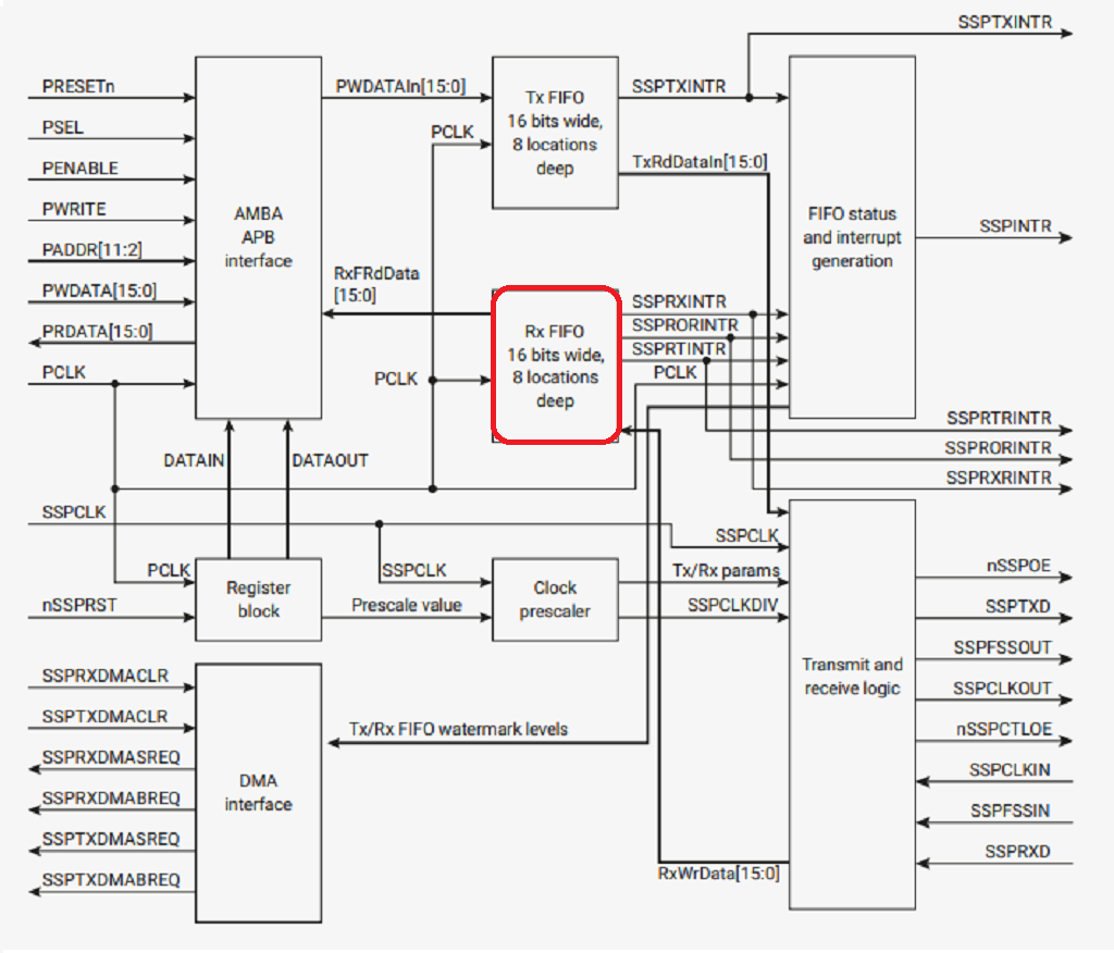
It is a 16-bit wide, 8-bit deep memory buffer.
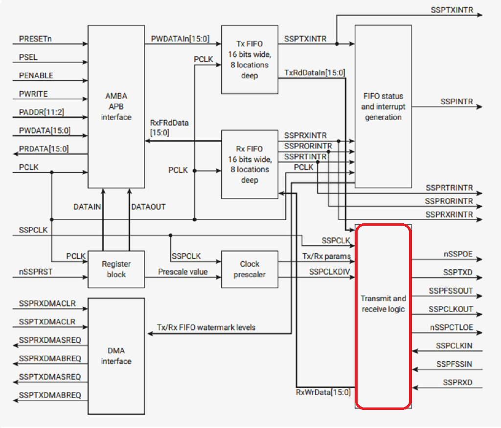
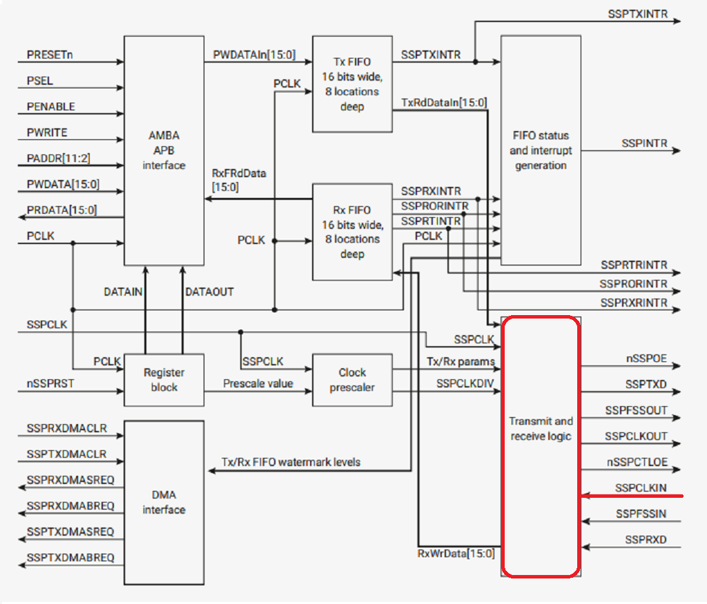
When the SPI is configured as the master device the clock signal is provided by its own clock divider.
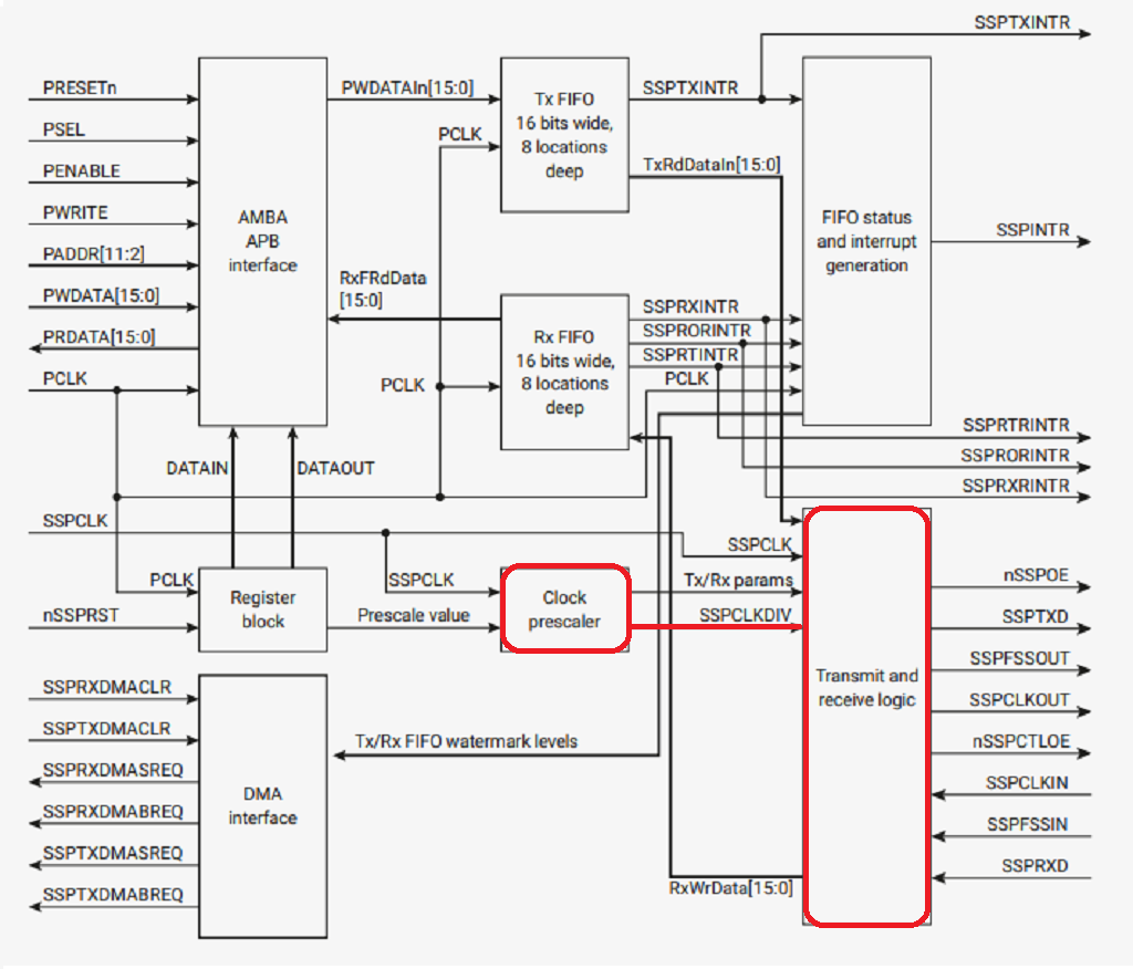
Conversely, the clock signal is provided externally.
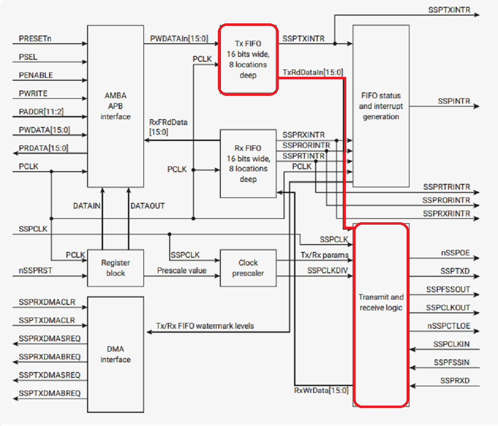
When data needs to be transferred, the transfer logic block reads a value from the transfer FIFO memory.
It is converted to serial data and output according to the clock signal.
The receive logic block receives the data according to the clock signal and stores it in the receive FIFO so that it can be read by the APB interface.
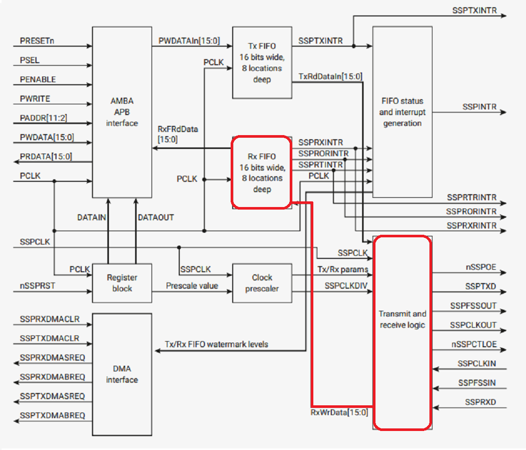
so that the APB interface can read
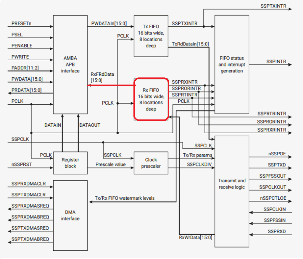
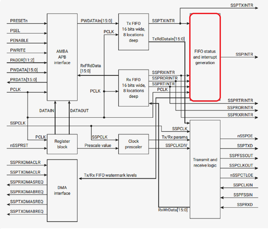
PrimeCell can generate 4 independent maskable interrupts, which are output via a combined interrupt.
1.6.1machine.SPl(id,baudrate,polarity,phase,bits,firstbit,sck,mosi,miso)
id: SPI object constructor, used to initialize the corresponding channel and pin parameters id is the SPI channel used, can be 0 or 1.
baudrate: The SPI communication rate, i.e. the frequency on the SCK pin.
polarity: clock polarity, if 0, SCK outputs low when the bus is idle, and vice versa.
phase: the phase of the clock, if 0 the data is captured on the first clock edge, and vice versa on the second clock edge.
bits :The number of bits of data to be transferred at a time.
firstbit: whether the high bit or the low bit is transmitted first.
sck, mosi and miso are all pins used by SPI and should be Pin objects.
The init function, used to restart the SPI.
The deinit function, used to shut down the SPI.
The read function, used to read data from the device and return it, with the parameter nbytes being the number of bytes read.
write: When reading data, MOSI outputs the data.
readinto function, used to read the data from the device and store it in the specified character array.
buf is an array of characters used to store the received data.
write: When reading data, the MOSI outputs the data.
The parameter buf is an array of characters, which is used to store the data to be transferred.
The write_readinto function, which is used to send and receive data at the same time.
write_buf: Array of characters to hold the transmitted data.
read_buf: an array of characters to hold the received data.
PS: The length of the character arrays for transmitting and receiving data must be the same.
from machine import SPI,Pin
import time

spi = SPI(1,baudrate=5_00e_000,sck=Pin(10) ,mosi=Pin(11) ,miso=Pin(12))
IRQ= Pin(17,Pin.IN)
TP_CS =Pin(16,Pin.oUT)
TP_CS(1)


while True:
    if IRQ() == 0:
        TP_CS(0)
        spi.write(bytearray ( [0xD0]))
        Read_date = spi.read(2)
        time.sleep_us(10)
        x_Point=((Read_date[e]<<8)+Read_date[1])>>3

        spi.write(bytearray( [ex90]))
        Read_date = spi.read(2)
        Y_Point=((Read_date[e]<<8)+Read_date[1])>>3
        TP_CS(1)

    time.sleep(0.5)


