

PIO is a new type of hardware developed for the RP2040 that can be used to create new or additional hardware interfaces on RP2040-based devices.
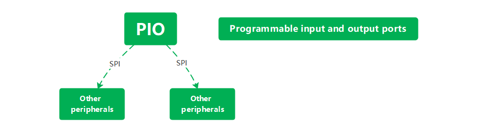
However, what is its role? It is essentially close to an FPGA, which is a field-programmable logic gate array that emulates all interfaces through a simple state machine, provided of course that the corresponding clock frequency is met.

If you explain it this way, you may still not understand the following scenarios:
Scenario 1: You need to use some communication interface, but the current peripherals can not meet your needs.

Scenario 2: You need to use certain interfaces such as single bus protocol, VGA, DVI, etc., but the RP2040 has no ready-made peripherals.

In the above scenarios, we can create the interface we need to meet the corresponding requirements through PIO customization.

Unlike software emulation, PIO does not take up kernel time.

Because each PIO has four independent state machines, ultra-high speed and programmable inputs and outputs can be achieved.

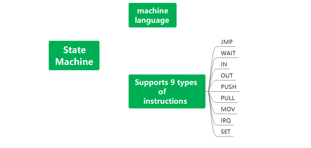
A state machine can be thought of as a minimalist kernel that can only be used to process specific instructions to achieve specific functionality.

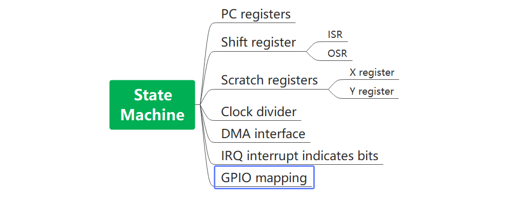
The RP2040 has two PIO blocks, each consisting of four state machines and instruction registers, which can independently execute sequential programs to operate the GPIOs and transfer data. Unlike general-purpose processors, the PIO state machine is highly focused on IO control and precise clock control.

Each state machine is equipped with a 32-bit PC register, used to point to the address of the instruction being executed, the shift register as the name implies data can be moved in it, and here the shift register can be directly transferred with the corresponding FIFO memory data in the following FIFO memory will be replaced by the English abbreviation FIFO.

Two 32-bit temporary storage registers, called X-register and Y-register.

There are 4×32-bit bus FIFOs in the receive and transmit directions.

A 16-bit integer, 8-bit decimal fractional clock divider, the input clock is the system clock, and the minimum state machine clock can be reduced to 65536 parts per second of the system clock.

DMA interface with sustained throughput of up to 1 word per system clock, with a maximum throughput of 100M words per second if the system clock is 100Mhz.

IRQ interrupt bits, PIO has a total of 8 interrupt bits that can be used to synchronise the state machine or for other purposes.

Each state machine can be flexibly GPIO mapped in four ways: input mapping, output mapping, setting mapping and sideloading.
Here we need to understand the GPIO mapping in more detail, in order to help us better understand PIO first we need to know that the mapping registers are 32 bits, if we let its one bit corresponds to a GPIO pin, we should use 32 GPIO pins corresponding.
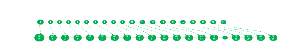
That is, the RP2040 has only 30 GPIOs and we should assume that it has 32 GPIOs, i.e. GPIOs 30 and 31.
We can also jokingly call this “disappearing pins” This knowledge is important and we will face it again and again for the input mapping, where we can specify the initial pins of the input GPIOs.
We can specify the initial pin of the input GPIO, this initial pin will be considered as pin 0 in the PIO input map and the other pins will be counted in order (cyclic), here we will encounter the “disappearing pin”. If GPIO29 is set as the initial pin, which is pin 0, and then incremented through GPIO30 and GPIO31, pin 3 corresponds to GPIO0.
Output mapping is similar to input mapping, but requires setting the number of output pins up to 32.
Set and side mapping works in the same way as output mapping, but up to 5 lO’s are mapped, set and side mapped pins are allowed to overlap.
It was previously introduced that the state machine is similar to a minimalist kernel, and only allows very simple binary programs. It is written in PIO assembly that is close to machine language. It supports 9 kinds of instructions: JMR, WAIT, IN, OUT, PUSH , PULL, MOV, IRQ, SET.
The PIO ASM programs we write are compiled by the compiler into the corresponding instructions and then given to the PIO’s state machine to run.

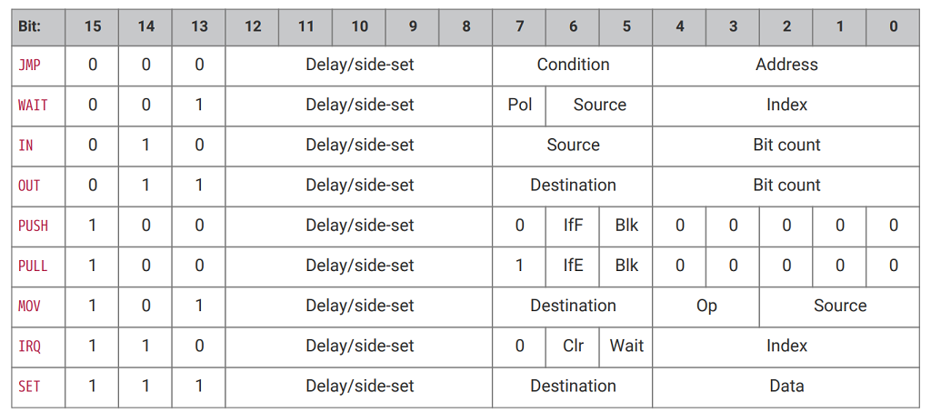
First we see the PIO instruction code table, which helps us to understand the relationship between the PIO ASM instructions and the parameters.
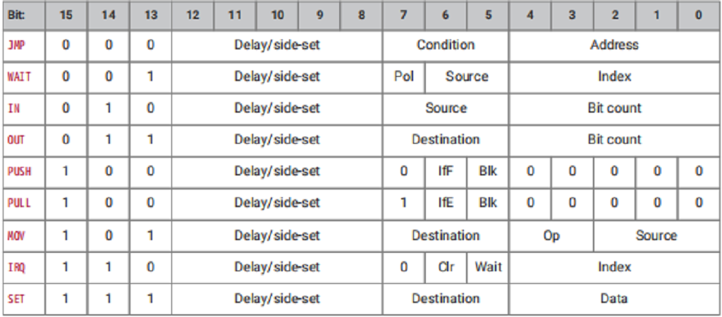
You can see that the length of an instruction is 16 bits.
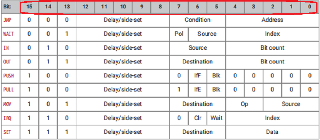
The high three digits are used to identify the function or effect of this instruction.
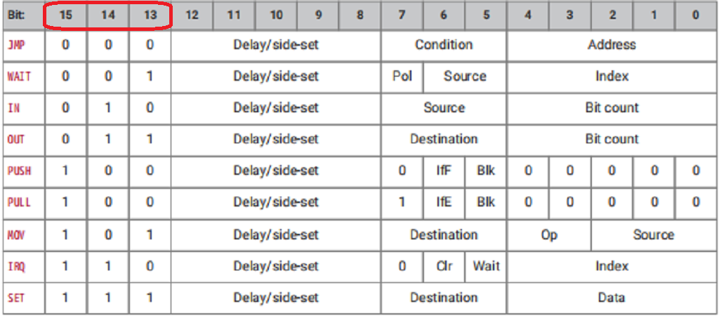
Bits 12-8 are used to identify delays or sideloads, while bits 7-0 will have different functions depending on the instruction.
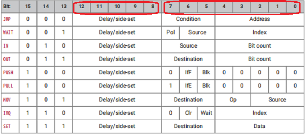
The purpose of the JMP instruction is to jump the program to the specified address if certain conditions are met.

The JMP directive has two parameters, condition, and target.

target :Allowed values 0-31, because PIO only has 32 instruction space
condition : !X OR!Y:X,Y register is 0
X–OR Y–:X,Y register minus l is greater than 0X!=Y :X is not equal to Y
PIN :input pin is high
! (OSRE): Input shift register OSR is 0
When the program is reached, the program will jump to the specified address according to the target, or, of course, it will jump to the specified address unconditionally if the condition is not filled in.
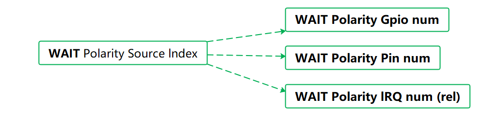
The WAIT instruction acts as a wait before the condition is met.

The WAIT command has three parameters, Polarity, Source and Index pointer.
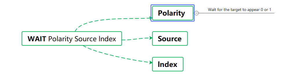
Polarity means waiting for a 0 or 1 to appear on the target.
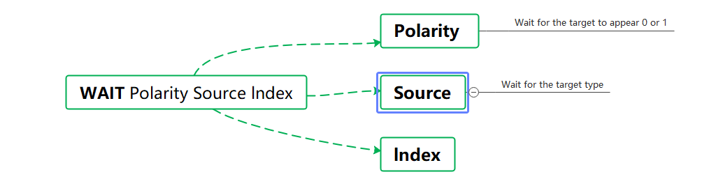
The source refers to the type of target to wait for, which can be absolute GPIO, PIN after pin mapping and the interrupt flag IRQ.
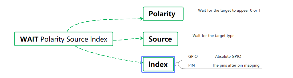
The source pointer corresponds to the type of target to wait for, which can be absolute GPIO, pin mapped PIN and interrupt flag IRQ, and the pointer corresponds to the target code to wait for.
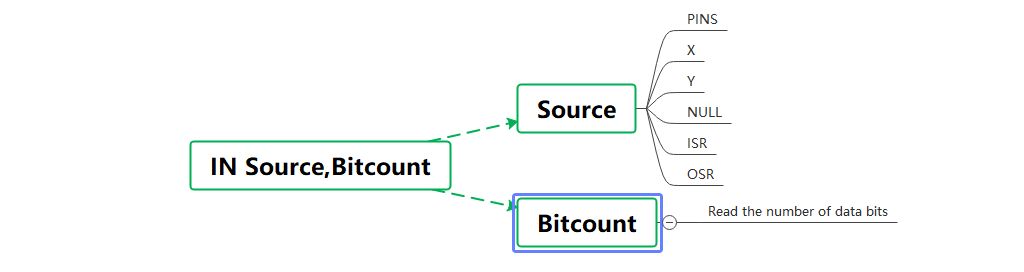
The function of the IN instruction is to store the data in the ISR register.

The IN instruction has two parameters, the Source and the Bitcount.

Source means the source type corresponding to the readout data.

The number of bits corresponds to the number of bits of data to be read.
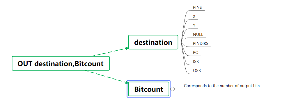
The OUT instruction is the opposite of the IN instruction in that it outputs the OSR to the target.

The OUT command has two parameters destination target and bitcount.

The target corresponds to the target of the data output and can be one of the following.
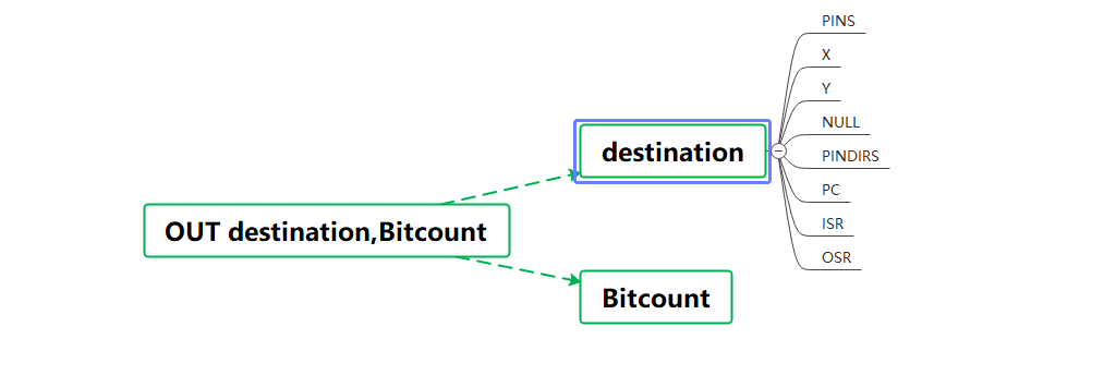
The number of bits corresponds to the number of output bits.
The PUSH instruction pushes the contents of the ISR into the RX FIFO and clears the ISR.

It has two parameters: full and blocking, if full is 1 then the ISR reaches the threshold before pushing.
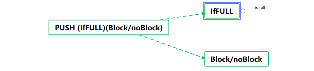
If blocking is 1 and the RX FIFO reaches the threshold, the data will be pushed into the ISR register, otherwise it will wait for the RXFIFO to reach the threshold, if it is 0 then the RXFIFO will not be pushed if it does not reach the threshold.
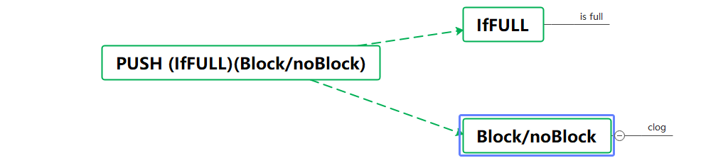
The PULL instruction reads the data from the TXFIFO into the OSR register.

It has two parameters, null and blocking.

If empty is 1, the TXFIFO threshold is reached before the OSR will receive data from the TXFIFO.

The blocking is the same as the blocking in PUSH, so we won’t – go over it.
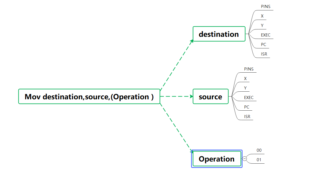
The function of the MOV instruction is to move data from the source to the destination register.

It has three parameters: target, source and operation.

The target is the register to which the data will be written, which can be one of the following.
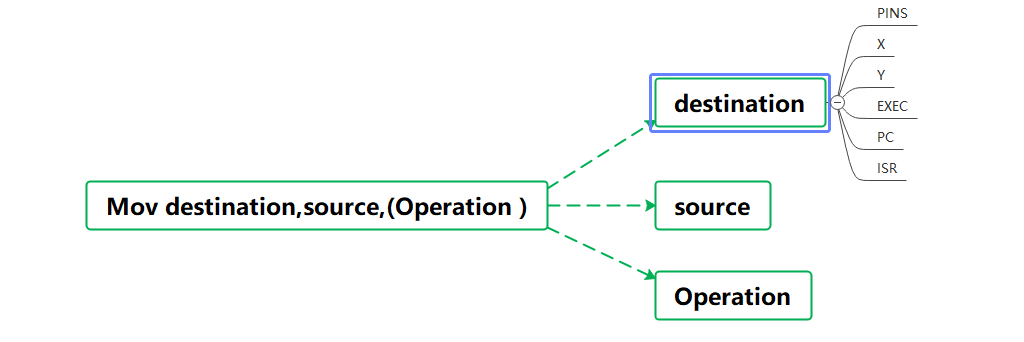
It is important to note that the EXEC decoder register, which is used to read an instruction from an external source and execute it, is theoretically capable of executing external PIO code.
The source is the data source, which can be one of the following.
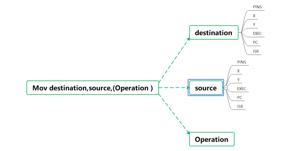
There are three types of operation, 00 for no change, 01 for dark bit reversal, 10 for bit flip, and high and low bit swap.
The IRQ instruction is used to set or clear the interrupt flag.

It has three parameters: options, interrupt flags and REL.

The options are as follows.
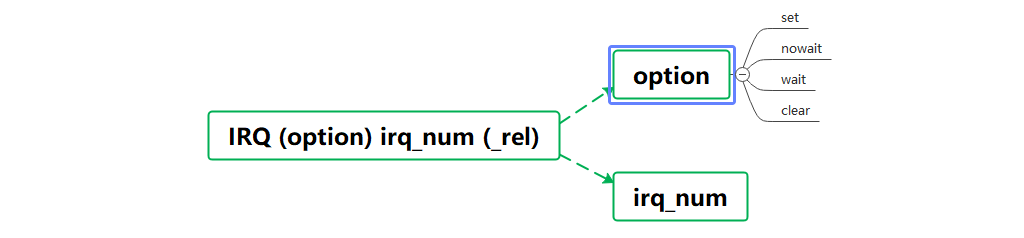
The interrupt marker can be 0 to 7.
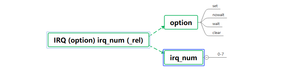
If rel exists, the interrupt identifier irq_num and the state machine code sm_num are added modulo 4. If state machine 2 sets interrupt identifier 0X11, the last interrupt value is 0X03.
The target is the register or pin to which the data is to be written.

The target is the register or pin to which the data is to be written.

The data is the data written, here only absolute values are possible.

These are the 9 instructions of the PIO ASM, but if you have seen the PIO ASM program, you will see that the instructions are followed by a few small trails.

For example, with a number in square brackets.

This stands for delay. In a normal program, each instruction takes 1 clock cycle to execute, but often we need to wait or we don’t need to go that fast, so we need to do a delay.

There are now two ways to do this:
1. Use a nonsense instruction, which assigns the value of the y register to the y register, which is a nonsense instruction.

But it takes up one clock cycle of the state machine. It has the disadvantage that it takes up the instruction space of the PIO, because the instruction space of the state machine can only hold 32 instructions, so it is not recommended to use this method.

2. Latency characteristics using PIO ASM

This instruction sets pins to 1 and then delays it by 2 clock cycles, which is the delay feature of the pio assembly.

The delay time is of course also characteristic, with a maximum delay time of 31 clock cycles.

By the way, we would like to introduce another interesting and useful feature of the PIO ASM.

By the way, there is another interesting and useful feature of the PIO ASM.
Any instruction can be executed while changing the mapped pins set as side preserves, up to a maximum of 5 pins, a point to be noted here as we can see in the PIO instruction code table.
Sidesets and delays are 12-8 bits of a shared instruction.
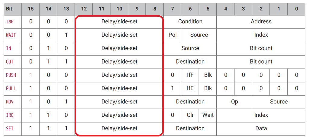
So side-positioning and latency are not perfectly compatible but can be set to suit your own needs. As we said before the maximum value of latency is 31, which translates to 5 bits in binary.

That is, we cannot distinguish between delay and sideloading by coding, so we need to specify in the program that we are using sideloading bits.

Now let’s take a look at the routines.

This program will simulate the process of SPI sending data, and it will continuously output the values in the OSR registers (in order) through the pins corresponding to the pins.

At the same time the side-set pins will be constantly flipped to achieve two clock cycles to output one bit of data and output the clock signal, making our program smaller and faster.
This means that our Delay can only take up 4 bits, which means that its value ranges from 0-15.

A little extra mention of program packaging.
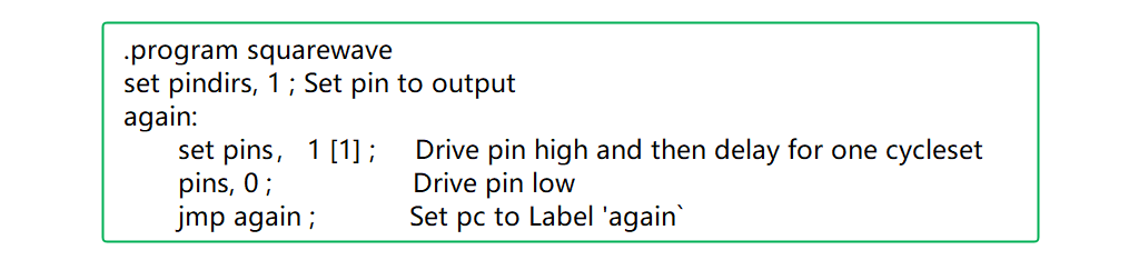
The program will start with the instruction at address 0, run until the instruction at address 31 is finished, then repeat from address 0. Next is a program that sets a pin to output and cycles through a square wave with a duty cycle of 50% and a period of 4 clock cycles.
This is a very common program where the PC pointer does not go back and forth between 0 and 31, so pio introduces a program wrapper that tells our state machine where to end and where to start again.
Now we can see the example program.
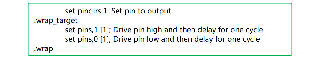
When the program runs to .wrap, it will return to .wrap_target and run. The difference with the previous program is that you don’t need to use the jump instruction to jump, which saves a single instruction.
Okay, that’s the end of the PIO syntax.
MicroPython introduced a new @rp.2Asm_pio decorator and rp2.PIO class.

The definition of the PIO program and the assignment of the state machine can be divided into 2 logical parts.
The pin mapping is bound to a pin and a state machine is assigned to execute a specific program, all program configurations such as Autopull are done through the decorator.

A decorator is essentially a function that allows other functions to add extra functionality without any code changes.
Now let’s look at the arguments to the asm_pio decorator, which are as follows.

The first three parameters are the output pin initialisation, the set pin initialisation and the side pin initialisation, which can be set to output high and output low.
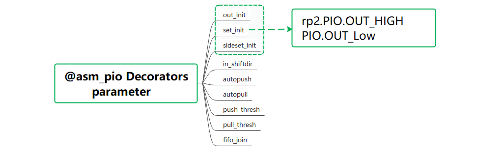
It is important to note that MicroPython uses the side pin initialisation to calculate how many side pins are used and to determine the structure of the side and delay fields.
The next two parameters are the data-in direction and the data-out direction.

It determines the direction of data movement, e.g. in the case of output, if the data is moved to the left, the high bit of the OSR is output first. If the data is moved to the right, the lower bit is output first.
The 6th and 7th parameters are auto-push and auto-pull, if enabled, the ISR or OSR will pull the corresponding data from the corresponding FIFO or push the data to the corresponding FIFO when the threshold value is reached.

The 8th and 9th parameters are the push and pull thresholds,these two parameters are literally used in combination with the automatic push and pull.
The last parameter is a FIFO combination, specifying a FIFO, closing another FIFO and adding it to the specified FIFO to get a deeper bit FIFO, if we specify a TXFIFO, we get a TXFIFO of 8 bits depth.

MicroPython uses PIO as a state machine, so our functions are all based around it.

The constructor is as follows.

sm_id:use state machine ID,0-3 for PIO0,4-7 for PIO1
program:state machine running program
freq: frequency of the state machine, default is the system clock frequency
ps: the allocation factor of the clock divider is calculated by the formula “system clock frequency/frequency”, so there may be a slight error
in_base: used for the first pin of the in() instruction out_base: used for the first pin of the out() instruction set_base: used for the first pin of the set() instruction jmp_pin: used for the first pin of the jmp(pin,…) instruction the first pin of the sideset_base instruction: is the first pin used for sidelining
SHIFT_LEFT or PIO.SHIFT_RIGHT out_shiftdir: the direction the OSR will move, can be PIO.
push_thresh: the push threshold
pull_thresh: pull threshold
function active: get or set whether the state machine is currently running, when value is not empty, set the state machine, and vice versa to get the running state.
The restart function restarts the state machine and jumps to the beginning of the program.
The parameter instr: is the command string.
The Get function takes a word from the rx fifo of the state machine. If the rx fifo is empty, it blocks until the data arrives (i.e. the state machine pushes a word).
put: Pushes a word into the TX FIFO of the state machine, if the FIFO is full it will block until space is available (i.e. the state machine pulls a word)
shift: shift the number of bits left before pushing
Returns the number of words in the RX FIFO of the state machine, a value of 0 means the FIFO is empty and is used to check if the data is waiting to be read before calling StateMachine.get()
Use the above knowledge points to drive the WS2812B to achieve autonomous control of the colour of the lamp column.
WS2812B is a single-bus driven control circuit and luminous circuit in one intelligent external control LED light source intelligent external control LED light source.
Single line output can be used to synchronise the output action by connecting the LEDs in series; – The data protocol uses a unipolar zeroing code.
Because of the internal integrated control circuit, the display is more delicate and smooth, solving the problem of dark streaks in the shooting screen; – Data transmission speed up to 800Kbps.
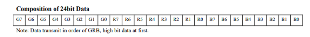
Here we can see that the communication protocol of the WS2812 is not the same as the communication protocols we have come across before.
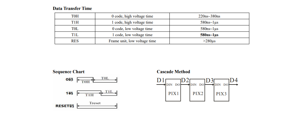
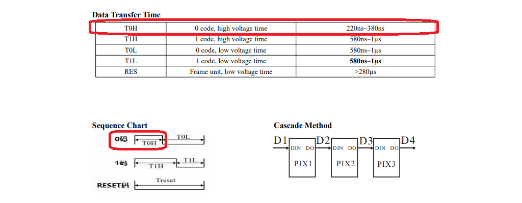
It is the duration of the level that determines whether the data is 0 or 1. If we need to send data 0, first pull the level high 220ns-380ns followed by the level low 580ns-1us.
The same principle applies to data 1.
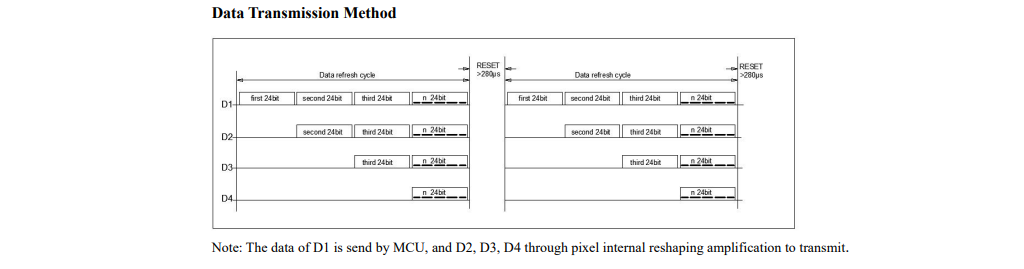
The ws2812 transmits data as shown in the table, and the ws2812 sends the data high first, i.e. the data is shifted to the left.
Here we have borrowed from the official WS2812B procedure for using the PIO driver.
Python
# Example using PIO to drive a set of WS2812 LEDs.

import array, time
from machine import Pin
import rp2

# Configure the number of WS2812 LEDs.
NUM_LEDS = 10
PIN_NUM = 22
brightness = 0.2

@rp2.asm_pio(sideset_init=rp2.PIO.OUT_LOW, out_shiftdir=rp2.PIO.SHIFT_LEFT, autopull=True, pull_thresh=24)
def ws2812():
    T1 = 2
    T2 = 5
    T3 = 3
    wrap_target()
    label("bitloop")
    out(x, 1)               .side(0)    [T3 - 1]
    jmp(not_x, "do_zero")   .side(1)    [T1 - 1]
    jmp("bitloop")          .side(1)    [T2 - 1]
    label("do_zero")
    nop()                   .side(0)    [T2 - 1]
    wrap()


# Create the StateMachine with the ws2812 program, outputting on pin
sm = rp2.StateMachine(0, ws2812, freq=8_000_000, sideset_base=Pin(PIN_NUM))

# Start the StateMachine, it will wait for data on its FIFO.
sm.active(1)

# Display a pattern on the LEDs via an array of LED RGB values.
ar = array.array("I", [0 for _ in range(NUM_LEDS)])

##########################################################################
def pixels_show():
    dimmer_ar = array.array("I", [0 for _ in range(NUM_LEDS)])
    for i,c in enumerate(ar):
        r = int(((c >> 8) & 0xFF) * brightness)
        g = int(((c >> 16) & 0xFF) * brightness)
        b = int((c & 0xFF) * brightness)
        dimmer_ar[i] = (g<<16) + (r<<8) + b
    sm.put(dimmer_ar, 8)
    time.sleep_ms(10)

def pixels_set(i, color):
    ar[i] = (color[1]<<16) + (color[0]<<8) + color[2]

def pixels_fill(color):
    for i in range(len(ar)):
        pixels_set(i, color)

def color_chase(color, wait):
    for i in range(NUM_LEDS):
        pixels_set(i, color)
        time.sleep(wait)
        pixels_show()
    time.sleep(0.2)

def wheel(pos):
    # Input a value 0 to 255 to get a color value.
    # The colours are a transition r - g - b - back to r.
    if pos < 0 or pos > 255:
        return (0, 0, 0)
    if pos < 85:
        return (255 - pos * 3, pos * 3, 0)
    if pos < 170:
        pos -= 85
        return (0, 255 - pos * 3, pos * 3)
    pos -= 170
    return (pos * 3, 0, 255 - pos * 3)


def rainbow_cycle(wait):
    for j in range(255):
        for i in range(NUM_LEDS):
            rc_index = (i * 256 // NUM_LEDS) + j
            pixels_set(i, wheel(rc_index & 255))
        pixels_show()
        time.sleep(wait)

BLACK = (0, 0, 0)
RED = (255, 0, 0)
YELLOW = (255, 150, 0)
GREEN = (0, 255, 0)
CYAN = (0, 255, 255)
BLUE = (0, 0, 255)
PURPLE = (180, 0, 255)
WHITE = (255, 255, 255)
COLORS = (BLACK, RED, YELLOW, GREEN, CYAN, BLUE, PURPLE, WHITE)

print("fills")
for color in COLORS:
    pixels_fill(color)
    pixels_show()
    time.sleep(0.2)

print("chases")
for color in COLORS:
    color_chase(color, 0.01)

print("rainbow")
rainbow_cycle(0)