

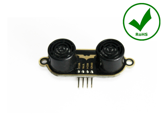
BAT – Ultrasonic Sensor Distance Measuring
January 10, 2019
The 3D Printer Record 2: Step Losses
January 10, 2019
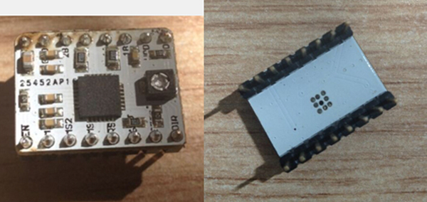
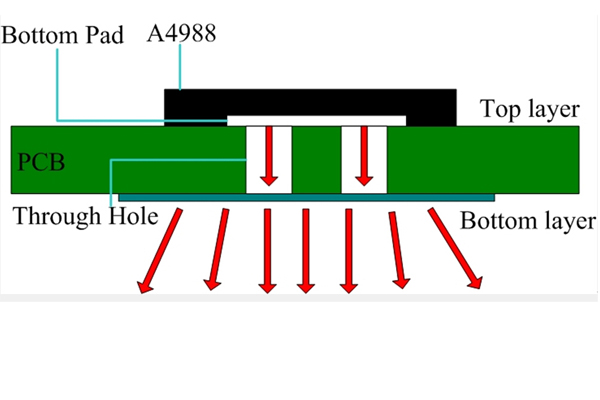
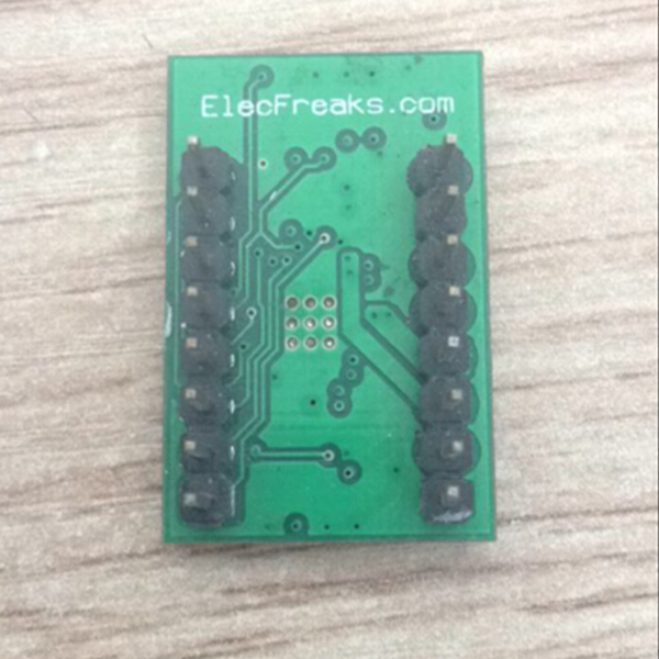
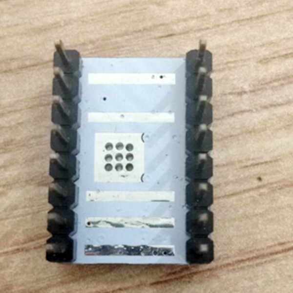
A4988 stepper motor driver does play a very important role in the 3D printer owing to the fact that its performance directly affects the printing accuracy, print quality, and stability. Since our motherboard uses a 24V stepper motor driver, A4988 driver chip generates much more heat than a 12V motor. Therefore, the design of an A4988 circuit with good heat dissipation to allow steady work is the focus of the entire work. The initial version of A4988 driver generated growing heat and had difficulties in cooling and long-time work. A4988 driver module has undergone generations of evolution with the first generation limited to only a few hours output of 100mA driver current. Now to our great satisfaction, it supports stable 400mA current output for over 24 hours. In the following part, we will share some of the experiences we have accumulated in the process with you. A4988 dissipates heat mainly through the bottom bonding pad, which must require punching for cooling. Our initial version is a two-board design with 9 through holes, 0.6mm as their diameter on the bottom layer, aiming to transfer heat to the bottom copper sheet through the 4 through holes and disperse it.
Schematic Diagram
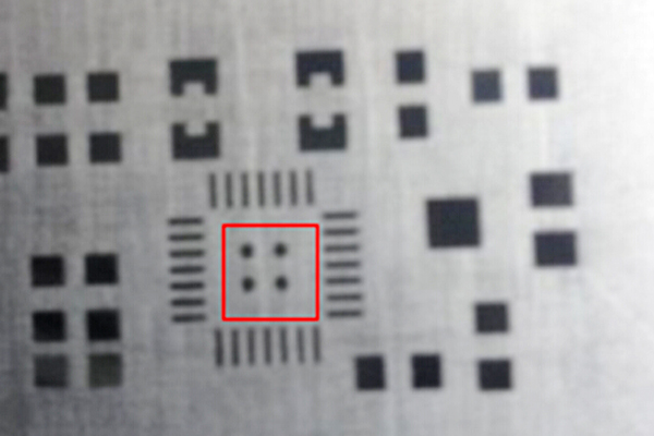
After testing, the cooling effect was not so ideal, so we further increased the size of the through holes to 0.8mm as diameter. Another round of testing showed that the cooling effect was significantly improved. So we concluded that if we want to further enhance the cooling effect, we should widen the copper area as much as possible. In order to achieve this effect, we changed the 2-layer PCB into 4-layer and put the layout into the inner layer to free up space large enough for the bottom copper sheet to dissipate heat. Explosion of the bottom copper part can help get a better cooling effect. For 2-layer PCB circuit, the layout has to be placed on the bottom layer.
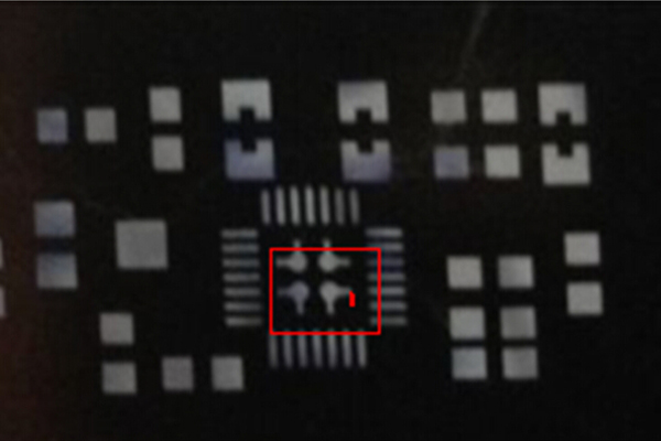
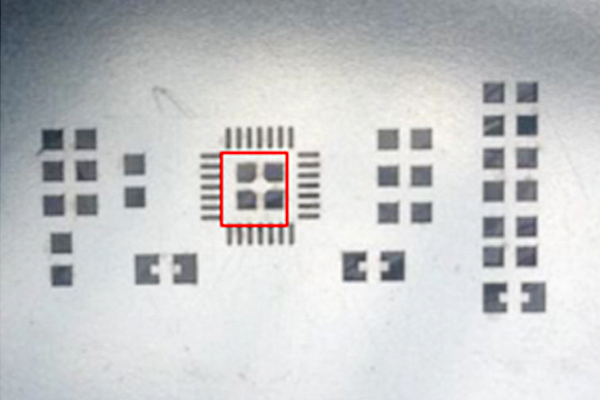
The picture below showcases a 4-layer PCB without layout on the bottom layer. The maximized copper area, plus pad expose Cu can greatly optimize the cooling effect.
But this was just not enough, extra attention needed to be given to production. As earlier versions of our PCB design were out of question, but some exceptions with bad cooling effect. After analysis, problems occurred in the section of solder paste. The amount of solder paste screen printed onto the bottom pad varied, thus, a proper amount was necessity for fine contact between the welded surface and PCB soldering, and ideal cooling effect. That’s why we improved the solder paste stencil and enlarged the window of the bottom bonding pad: once in a case of full solder paste, the best cooling effect can be obtained.
Earlier Solder Paste Stencil
Improved Solder Paste Stencil
Final Version Solder Paste Stencil
Here is a set of comparative data:
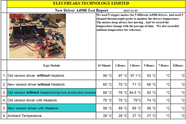 This set of data was measured under strict control of equivalent indoor temperature, motors and driver current.
Old version driver without heatsink.
This is the earliest 2-layer board, using the above stencil firstly mentioned. The soldering between A4988 bottom bonding pad and PCB is not strong enough. You can see that the temperature reaches as high as 98???
New version driver without heatsink.
This is the improved four-layer board, using the final version stencil. The soldering between A4988 bottom bonding pad and PCB is firm, which brings forth excellent heat dissipation. You can see the thermal performance is far better than the 2-layer board; the maximum value is only 71??? 27???lower than the earliest version.
Old version without heatsink (improve production process).
This is still a 2-layer board but with the final solder paste stencil and firm soldering between A4988 bottom bonding pad and PCB. The cooling effect, compared column “1” has greatly improved. You can see clearly that the maximum is only 84.5 ??? 12 ???lower than column “1”, but 13.5 ???higher than the 4-layer board version. Statistics in column 4 and 5 summarize results on 2-layer board and 4-layer board respectively, both with heatsink added. The maximum temperature for the later is only 65 degrees Celsius, a value low enough to meet our thermal design requirement. Hence, we decided to adopt a 4-layer design. To make a short summary of the above practices, we should pay attention to a few points regarding the A4988 thermal design.
- It’s necessary to place through holes onto the bottom bonding pad. The larger the holes are, the better.
- A broad enough bottom cooling copper sheet and 4-layer design are suggested. You’d better place the layout into the inner layer and copper exposed to better heat dissipation.
- The solder paste stencil window at the bottom should be large enough. The solder paste must be fully printed and ensure that the soldering between the bottom bonding pad and the PCB is solid.
Just follow these few points, you can get a good heat dissipation. But note that increasing the driver current again and again will make A4988 overburdened, as a consequence, tremendous heat will be generated which cannot be easily dissipated in time. Therefore, to choose a suitable driver current is also particularly important, then how to choose the right driver current of it?